AMD announced on August 6 that it plans to acquire Taalas, a Toronto-based startup that builds AI model weights directly into silicon. The deal targets a persistent cost in running AI models: repeatedly moving billions of parameters from memory to the hardware that performs the calculations.
Taalas's approach gives up some of a GPU's flexibility to reduce that movement. Its HC1 chip is built for a specific model, with weights permanently encoded during manufacturing. The company reports that HC1 can serve Meta's Llama 3.1 8B at 16,960 tokens per second. Those are vendor benchmark results, but they make the technology worth examining, along with the constraints that come with a model-specific chip.
As of August 7, the acquisition hasn't closed. Terms are undisclosed, and completion is expected in Q4 2026, pending regulatory approval.
Why moving weights costs so much
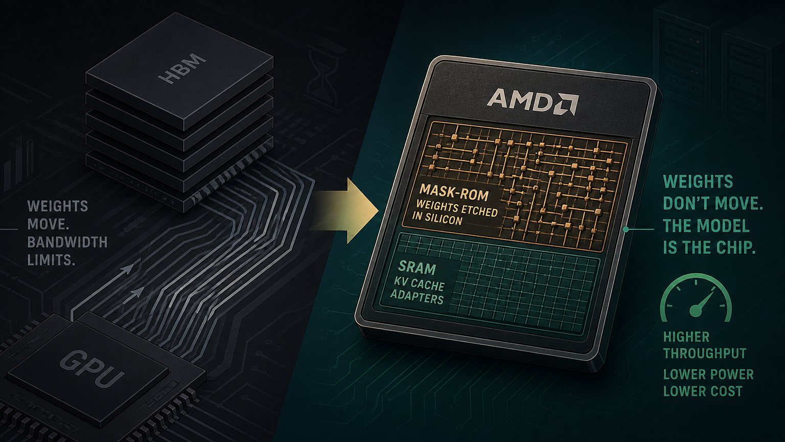
During transformer token generation, the same model weights are used repeatedly to calculate each next token. In the GPU execution pattern described here, weights move from high-bandwidth memory, or HBM, into on-chip SRAM for each forward pass. SRAM is fast working memory located on the chip.
A 70-billion-parameter model using 16-bit floating-point weights contains 140 GB of weight data. Moving that much data across a memory bus delivering 3 to 4 terabytes per second takes time, even when the processor has plenty of arithmetic capacity. In memory-bound generation workloads, compute units can spend a substantial amount of time waiting for data.
Faster HBM helps. Nvidia's H200 provides 4.8 TB/s of HBM3e bandwidth, compared with 3.35 TB/s for the H100. But the basic arrangement still separates weight storage from compute. Each pass requires weight data to reach the units doing the calculations. More bandwidth reduces the cost of that movement without removing the need for it.
This is the architectural mismatch behind the case for Taalas: repeated generation with fixed weights may not need the same flexible hardware used to train a model or run many different models.
How HC1 stores a model
Taalas's HC1 is fabricated on TSMC's 6-nanometer process. According to the company's description, model weights are encoded in mask-ROM transistor structures, with metal connections set during manufacturing. The weights become a permanent part of the chip rather than a model that must be loaded from HBM at runtime.
The design has two distinct regions. A mask-ROM recall fabric holds the fixed model weights. An SRAM recall fabric holds runtime data, including the key-value, or KV, cache and fine-tuning adapters. The KV cache retains information from earlier tokens so the model can use that context during generation.
The claimed benefit is the removal of repeated weight transfers from external memory. That distinction matters: HC1 still needs runtime memory, but it doesn't use HBM to stream the model's weights through the processor on every generation step.
In its February announcement, Taalas reported 16,960 tokens per second for Llama 3.1 8B. At the time, it claimed 73 times the throughput of an Nvidia H200 at one-tenth the power. Reporting on the August 6 acquisition announcement gave updated comparisons of 48 times faster than Nvidia's GPUs and 8.5 times faster than Cerebras's accelerators.
These comparisons remain vendor claims. The earlier H200 comparison and the later, broader GPU comparison shouldn't be treated as interchangeable measurements. If gains of that size carry into production, however, they would materially change the cost and power requirements of serving a supported model.
Updating a model means changing silicon
The main constraint follows directly from the design. Permanently encoded weights can't be replaced by loading a new model file. A significant base-model update requires new silicon. Hardware deployed six months earlier can't simply switch to the revised weights.
Taalas offers two ways to make that constraint more manageable. LoRA-style adapters can be loaded into the SRAM fabric at inference time. These adapters allow deployment-specific fine-tuning without replacing the fixed base model.
For changes to the base model itself, Taalas claims that only two of the chip's more than 100 metal layers need to change between model versions. The company says its in-house tooling and streamlined tape-out process can produce silicon for a revised model in roughly two months. Tape-out is the step at which a chip design is finalized for manufacturing.
That is still a meaningful delay for an API provider whose customers expect new model versions immediately. A market with monthly model releases is a difficult fit for hardware that takes two months to revise.
The tradeoff looks more practical for services running stable production models at high volume. Llama 3.x variants, purpose-built fine-tunes, and services with locked model versions may remain useful long enough to justify dedicated hardware. The commercial bet is that this stable-model segment is larger, and growing faster, than attention to the newest model releases might suggest. That remains a judgment about the market rather than an established result.
Where Taalas fits into AMD's systems
AMD intends Taalas to complement its Helios rack-scale systems and Instinct GPUs. The proposed arrangement divides inference into two phases. Instinct GPUs handle prompt processing, usually called prefill, while Taalas chips handle token generation.
Prefill processes the input prompt and benefits from parallel computation across that input. Token generation repeatedly applies the same weights as the response grows. For workloads where prefill is compute-bound and generation is memory-bandwidth-bound, separate hardware for each phase could improve efficiency.
This split has a clear technical rationale. GPUs retain flexibility for variable-length inputs and general-purpose parallel work, while model-specific chips take on repeated generation with fixed weights. Whether the combined rack delivers the expected savings will depend on production performance and AMD's integration work.
Vamsi Boppana, AMD's senior vice president for the AI Group, said the Taalas technology and engineering team would strengthen AMD's portfolio through differentiated inference performance. Taalas co-founder and CEO Ljubisa Bajic pointed to AMD's scale and global reach as reasons for joining the company.
The acquisition also sits alongside AMD's Helios GPU cluster work and reported partnership conversations with Cerebras. Together, those efforts suggest a strategy that allows several approaches to inference acceleration. Different workloads may justify different hardware, rather than a single design replacing every other option.
Which deployments could benefit
For organizations running inference today, the announcement doesn't create an immediate purchasing decision. There is no commercial product to order and no HC2 specification sheet for the planned follow-on chip. The acquisition itself remains pending.
The most promising deployment profile is specific: a stable model, high request volume, and enough inference spending for hardware efficiency to matter. A fine-tuned production model served at scale could fit that profile, provided its required adaptations work within the chip's supported approach.
Rapid model iteration is a weaker fit. So are low-volume services and shared infrastructure serving many different model versions. In those settings, flexibility and hardware utilization may be more valuable than the efficiency available from a chip tied to one base model.
The stated HC2 roadmap targets 20 billion parameters per chip. Taalas also describes pipeline parallelism across 50 accelerators as a path to trillion-parameter models. Pipeline parallelism splits model processing across devices, with each device handling part of the work. These are roadmap targets, not available product specifications.
That plan extends the idea beyond a single 8-billion-parameter model. It also makes the economics depend on how long large production models remain stable. The more useful work a fixed model can perform before replacement, the easier it becomes to justify silicon built specifically for it.
What still needs to hold up
Flash attention, speculative decoding, quantization, and faster HBM address inference costs in different ways. They can reduce memory traffic or make better use of existing hardware, but they don't permanently encode the base model in the chip. Taalas takes a more restrictive approach in exchange for its claimed performance and power gains.
AMD's planned purchase is a bet that some inference workloads are stable and large enough to support that restriction. It doesn't establish that memory has disappeared from the inference workload, or that GPUs are no longer suitable for generation.
The unresolved tests are production-scale performance, integration into an AMD product, and demand for hardware tied to particular models. If HC1's benchmark gains carry into deployed services, dedicated generation hardware could become a more attractive counterpart to GPUs. For buyers, the useful comparison will be the cost of serving a supported model over its working life, including the delay and expense of replacing it when its weights change.